- 您现在的位置:买卖IC网 > Sheet目录3841 > PIC16F737-I/SP (Microchip Technology)IC PIC MCU FLASH 4KX14 28DIP
2009 Microchip Technology Inc.
DS39636D-page 223
PIC18F2X1X/4X1X
19.0 COMPARATOR MODULE
The analog comparator module contains two compara-
tors that can be configured in a variety of ways. The
inputs can be selected from the analog inputs multiplexed
with pins RA0 through RA5, as well as the on-chip volt-
age reference (see Section 20.0 “Comparator Voltage
Reference Module”). The digital outputs (normal or
inverted) are available at the pin level and can also be
read through the control register.
The CMCON register (Register 19-1) selects the
comparator input and output configuration. Block
diagrams of the various comparator configurations are
shown in Figure 19-1.
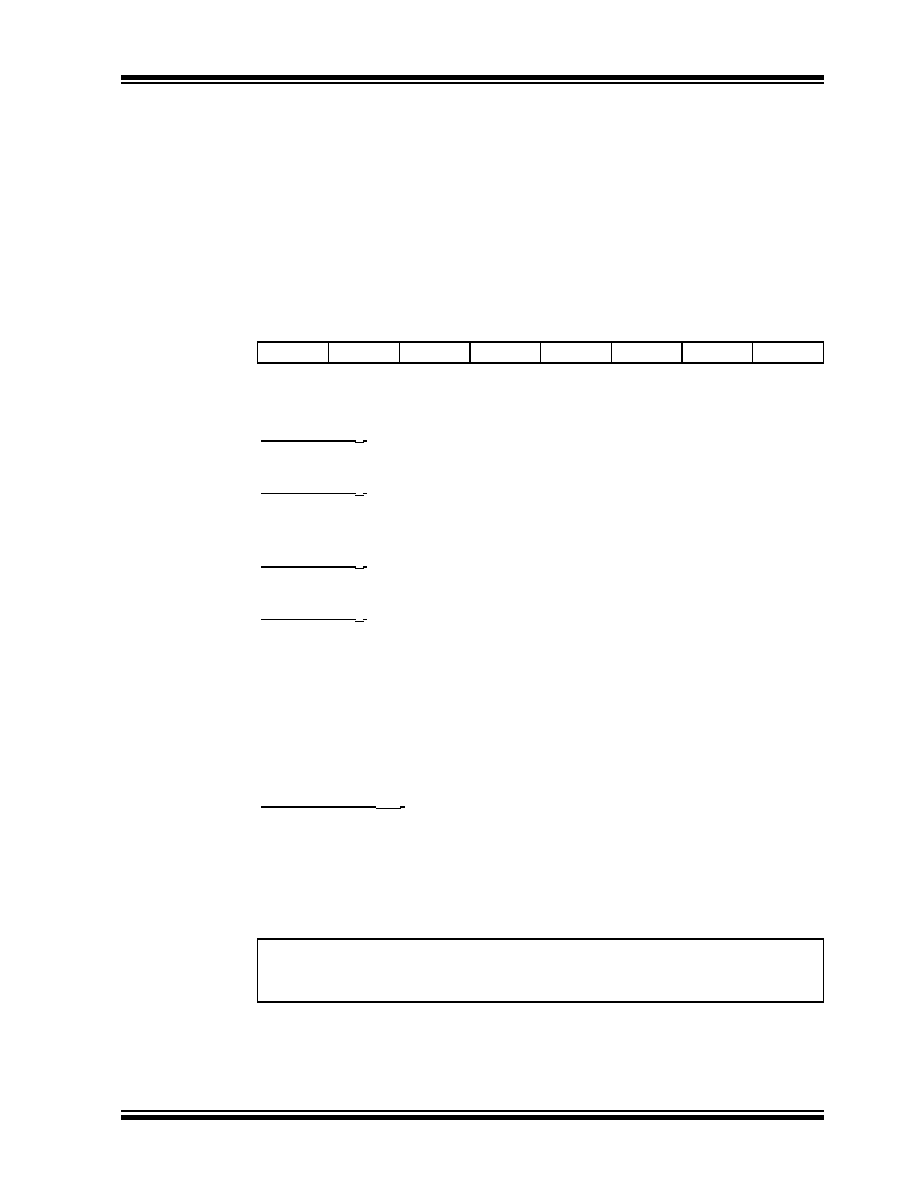
REGISTER 19-1:
CMCON: COMPARATOR CONTROL REGISTER
R-0
R/W-0
R/W-1
C2OUT
C1OUT
C2INV
C1INV
CIS
CM2
CM1
CM0
bit 7
bit 0
bit 7
C2OUT: Comparator 2 Output bit
When C2INV = 0:
1 = C2 VIN+ > C2 VIN-
0 = C2 VIN+ < C2 VIN-
When C2INV = 1:
1 = C2 VIN+ < C2 VIN-
0 = C2 VIN+ > C2 VIN-
bit 6
C1OUT: Comparator 1 Output bit
When C1INV = 0:
1 = C1 VIN+ > C1 VIN-
0 = C1 VIN+ < C1 VIN-
When C1INV = 1:
1 = C1 VIN+ < C1 VIN-
0 = C1 VIN+ > C1 VIN-
bit 5
C2INV: Comparator 2 Output Inversion bit
1 = C2 output inverted
0 = C2 output not inverted
bit 4
C1INV: Comparator 1 Output Inversion bit
1 = C1 output inverted
0 = C1 output not inverted
bit 3
CIS: Comparator Input Switch bit
When CM2:CM0 = 110:
1 =C1 VIN+ connects to RA3/AN3/VREF+
C2 VIN+ connects to RA2/AN2/VREF-/CVREF
0 =C1 VIN- connects to RA0/AN0
C2 VIN- connects to RA1/AN1
bit 2-0
CM2:CM0: Comparator Mode bits
Figure 19-1 shows the Comparator modes and the CM2:CM0 bit settings.
Legend:
R = Readable bit
W = Writable bit
U = Unimplemented bit, read as ‘0’
-n = Value at POR
‘1’ = Bit is set
‘0’ = Bit is cleared
x = Bit is unknown
发布紧急采购,3分钟左右您将得到回复。
相关PDF资料
PIC18F86K22-I/PTRSL
MCU PIC 64K FLASH XLP 80TQFP
PIC16C63A-04I/SP
IC MCU OTP 4KX14 PWM 28DIP
PIC16C63A-04I/SO
IC MCU OTP 4KX14 PWM 28SOIC
52559-2270
CONN FFC 22POS .5MM VERT ZIF SMD
52559-1870
CONN FFC 18POS .5MM VERT ZIF SMD
DSPIC33EP64MC506-I/PT
IC DSC 16BIT 64KB FLASH 64TQFP
52745-1896
CONN FFC 18POS .5MM R/A ZIF SMD
PIC16LC622-04/P
IC MCU OTP 2KX14 COMP 18DIP
相关代理商/技术参数
PIC16F737-I/SP
制造商:Microchip Technology Inc 功能描述:IC 8BIT FLASH MCU 16F737 SDIL28
PIC16F737-I/SS
功能描述:8位微控制器 -MCU 7KB 368 RAM 25 I/O RoHS:否 制造商:Silicon Labs 核心:8051 处理器系列:C8051F39x 数据总线宽度:8 bit 最大时钟频率:50 MHz 程序存储器大小:16 KB 数据 RAM 大小:1 KB 片上 ADC:Yes 工作电源电压:1.8 V to 3.6 V 工作温度范围:- 40 C to + 105 C 封装 / 箱体:QFN-20 安装风格:SMD/SMT
PIC16F737T-I/ML
功能描述:8位微控制器 -MCU 7KB 368 RAM 25 I/O RoHS:否 制造商:Silicon Labs 核心:8051 处理器系列:C8051F39x 数据总线宽度:8 bit 最大时钟频率:50 MHz 程序存储器大小:16 KB 数据 RAM 大小:1 KB 片上 ADC:Yes 工作电源电压:1.8 V to 3.6 V 工作温度范围:- 40 C to + 105 C 封装 / 箱体:QFN-20 安装风格:SMD/SMT
PIC16F737T-I/SO
功能描述:8位微控制器 -MCU 7KB 368 RAM 25 I/O RoHS:否 制造商:Silicon Labs 核心:8051 处理器系列:C8051F39x 数据总线宽度:8 bit 最大时钟频率:50 MHz 程序存储器大小:16 KB 数据 RAM 大小:1 KB 片上 ADC:Yes 工作电源电压:1.8 V to 3.6 V 工作温度范围:- 40 C to + 105 C 封装 / 箱体:QFN-20 安装风格:SMD/SMT
PIC16F737T-I/SS
功能描述:8位微控制器 -MCU 7KB 368 RAM 25 I/O RoHS:否 制造商:Silicon Labs 核心:8051 处理器系列:C8051F39x 数据总线宽度:8 bit 最大时钟频率:50 MHz 程序存储器大小:16 KB 数据 RAM 大小:1 KB 片上 ADC:Yes 工作电源电压:1.8 V to 3.6 V 工作温度范围:- 40 C to + 105 C 封装 / 箱体:QFN-20 安装风格:SMD/SMT
PIC16F73-E/ML
功能描述:8位微控制器 -MCU 7 KB 368 RAM 25I/O RoHS:否 制造商:Silicon Labs 核心:8051 处理器系列:C8051F39x 数据总线宽度:8 bit 最大时钟频率:50 MHz 程序存储器大小:16 KB 数据 RAM 大小:1 KB 片上 ADC:Yes 工作电源电压:1.8 V to 3.6 V 工作温度范围:- 40 C to + 105 C 封装 / 箱体:QFN-20 安装风格:SMD/SMT
PIC16F73-E/SO
功能描述:8位微控制器 -MCU 7KB 192 RAM 22 I/O RoHS:否 制造商:Silicon Labs 核心:8051 处理器系列:C8051F39x 数据总线宽度:8 bit 最大时钟频率:50 MHz 程序存储器大小:16 KB 数据 RAM 大小:1 KB 片上 ADC:Yes 工作电源电压:1.8 V to 3.6 V 工作温度范围:- 40 C to + 105 C 封装 / 箱体:QFN-20 安装风格:SMD/SMT
PIC16F73-E/SP
功能描述:8位微控制器 -MCU 7KB 192 RAM 22 I/O RoHS:否 制造商:Silicon Labs 核心:8051 处理器系列:C8051F39x 数据总线宽度:8 bit 最大时钟频率:50 MHz 程序存储器大小:16 KB 数据 RAM 大小:1 KB 片上 ADC:Yes 工作电源电压:1.8 V to 3.6 V 工作温度范围:- 40 C to + 105 C 封装 / 箱体:QFN-20 安装风格:SMD/SMT